Achieving High-Power-Density Design: Integrated Solutions with Advanced DC-DC Converters and Chip Resistors.
Achieving High-Power-Density Design: Integrated Solutions with Advanced DC-DC Converters and Chip Resistors.
1. The Imperative for Miniaturization in Modern Electronics
The relentless drive towards more compact, powerful, and efficient electronic systems, from data center servers to on-board chargers in electric vehicles, has made high-power-density a paramount design goal. This concept measures the amount of power that can be processed within a given volume. Achieving it requires a holistic approach that looks beyond individual component performance to focus on system-level integration. The challenge is twofold: not only must individual components like DC-DC converters and resistors become smaller, but their interaction—how they are placed on a PCB and how they thermally affect one another—must be optimized. Inefficient power conversion and bulky passive components are traditional barriers to miniaturization. Therefore, the synergy between advanced, highly efficient power conversion ICs and miniature, high-performance passive components like chip resistors becomes the critical path to overcoming these limitations and packing more functionality into shrinking form factors.
2. The Role of Advanced DC-DC Converters and Chip Resistors
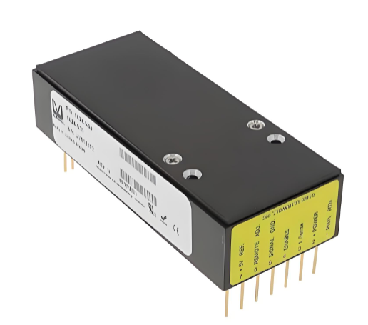
At the heart of high-power-density design are advanced DC-DC converters. These components have evolved from simple regulator modules to highly integrated systems-on-chip (SoCs) that incorporate power MOSFETs, gate drivers, and complex control logic. Key to their contribution is high switching frequency. By operating at frequencies reaching several megahertz, these converters drastically reduce the size of external passive components, particularly inductors and capacitors, which typically dominate the power solution's footprint. Complementing these converters are high-performance chip resistors. Components like thick film power chip resistors play vital roles in feedback voltage dividers, current sensing, and snubber circuits. For power density, their package size (e.g., 0402, 0201, or even smaller) is crucial. Crucially, resistors used for current sensing must offer low resistance values, low temperature coefficient of resistance (TCR) to maintain accuracy under thermal stress, and high power-handling capability per unit volume. This allows designers to place critical functionality closer to the converter without sacrificing performance or reliability.
3. Achieving Synergy through Co-Design and Layout Optimization
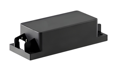
Simply selecting miniaturized components is insufficient; achieving true high-power-density demands co-design and meticulous PCB layout optimization. The high switching speeds of advanced converters make PCB layout parasitic inductance and capacitance a primary concern, as they can cause ringing, noise, and electromagnetic interference (EMI). The placement of chip resistors, especially for critical functions like current sensing, must be designed to minimize parasitic loop areas. Thermal management is the other critical aspect of integration. While efficient converters and resistors generate less heat, the concentrated power in a small area creates a high heat flux. A thermally optimized layout involves using thermal vias, copper pours, and sometimes metal cores to effectively dissipate heat away from both the converter IC and power-dissipating resistors. This prevents the formation of hot spots that could degrade performance or lead to premature failure. The ultimate goal is to create a compact, efficient, and thermally stable power stage where the converter and its associated passive components, like chip resistors, function as a single, highly optimized system.
Summary
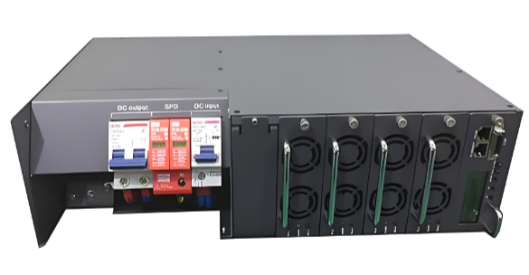
In conclusion, achieving high-power-density design is a multifaceted challenge that hinges on the synergistic integration of advanced DC-DC converters and miniature chip resistors. It requires a shift from viewing components in isolation to a system-level perspective that prioritizes high switching frequency, component miniaturization, meticulous PCB layout, and robust thermal management. This integrated approach is fundamental to developing the next generation of compact and powerful electronic equipment.

